
- 1pip安装模块警告InsecurePlatformWarning: A true SSLContext object is not available.
- 2Linux-sort排序_linux sort 排序 多条件排序
- 3阿里巴巴矢量图标如何使用_阿里巴巴矢量图标库怎么复制连接
- 47种常见的网络安全设备及其功能_常用的网络安全设备及其主要功能
- 5#创作纪念日# 我的创作128天纪念日_csdn代码片获得分享
- 6关于华为机试会不会考原题Od的问题?_华为机考是牛客网原题吗
- 7YOLOv8改进 | 卷积模块 | 在主干网络中添加/替换蛇形卷积Dynamic Snake Convolution_dynamic snake convolution based on topological geo
- 8Android wakelock 学习总结第三篇_android wake lock 与 kernel pm
- 9思科—计算机网络课程设计—第九章IPv4 NAT概念测试_下列哪种说法准确描述了动态 nat?
- 10Python:或且(与)非 : 逻辑运算和位运算_python且符号
FPGA DDR读写时序分析
赞
踩
FPGA DDR读写时序分析
使用Vivado中带的DDR的IP核可以方便进行DDR的读写,用户直接操控用户逻辑接口的信号,使信号满足时序逻辑即可。
具体时序逻辑请参照官方文档ug586_7Series_MIS.Pdf
下载链接:
https://china.xilinx.com/support/documentation/ip_documentation/mig_7series/v4_2/ug586_7Series_MIS.pdf
借鉴文章链接:
基于Xilinx MIS IP的DDR3读写User Interface解析
https://wenku.baidu.com/view/63e8c92d195f312b3069a5ea.html
命令路径:
官方文档时序:
app_rdy有效,从机已经处于等待接收状态,此时app_en有效,app_cmd和app_addr有效,则发送当前app_cmd中命令给DDR 控制IP。如果app_en有效,app_cmd和app_addr都有效,但是app_rdy处于忙状态,那么上面三个信号要保持有效状态,直到app_rdy处于空闲,即有效状态,才将命令发送给DDR控制IP。

DDR示例工程仿真:
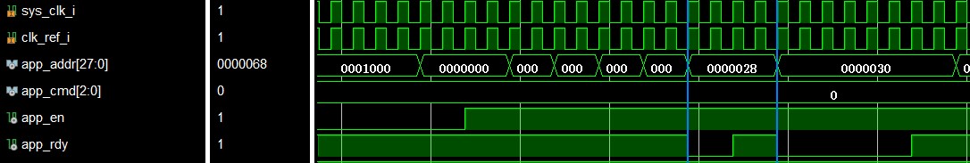
查看DDR IP的仿真,在第一个蓝色标志处上升沿,app_en有效,但是app_rdy处于忙状态,所以app_en保持高状态,app_cmd和app_addr保持有效状态,直到第一个蓝色标志处起第三个时钟上升沿app_rdy空闲,开始将app_cmd中指令发送给DDR IP控制器。第二个蓝色标志处也是一样,在蓝色标志处起第七个时钟,app_rdy空闲,发送app_cmd指令给DDR IP控制器。
写入操作:
官方文档时序:
当app_rdy和app_wdf_rdy为高时,app_en为高,则开始发送数据到write fifo中。

DDR示例工程仿真:
在写入时,app_rdy和app_wdf_rdy两个信号要处于有效状态。写入过程要写入128bit数据,共8个16bit数据,写入前6个数据时,app_wdf_rdy和app_rdy处于有效状态,在蓝色标注范围内,写第7个数据时,app_rdy为忙状态,所以第7和8两个数据并没有正常写入。

输入的命令和数据都有自己的FIFO用于存储,并且他们之间是同步的。数据比读写命令早或者晚写入都是可以的,因为他们在不同FIFO的同一层,同步时钟保证读写命令可以对应他需要操作的数据。如下所示,数据FIFO中只有一个3,对应着命令FIFO中的读,也就是会从FIFO中读个3出来,此时命令FIFO之后的写命令已经存进去了,但是数据FIFO与这些命令对应的操作数还没有写进去,但是即便是命令先写进去,数据后写进去也会写在响应命令对应的位置。数据比命令先写也是一样。

App_wdf_end信号,DDR3实际读写的Burst = 8。举例来说,DDR3的数据为宽为16bit,Burst为8,就是说每次对DDR3进行读写操作,必须是连续的8*16bit位数据。那么用户接口端,如果逻辑时钟为DDR3时钟的4分频,且数据位宽为128bit,那么单个时钟周期就应该对应Burst=8的一次读写操作;如果位宽为64bit,那么必须执行2次数据操作才能完成一次Burst=8的读写。对于前者app_wdf_end始终为1即可,对于后者app_wdf_end每2个写时钟周期内前一次拉低,后一次拉高。
App_wdf_data,app_wdf_wren和app_wdf_rdy,工作原理与命令路径类似。App_wdf_data有效,且app_wdf_wren拉高,必须app_wdf_rdy也为高,才表示当前数据写入DDR3 Controller IP。
读取操作:
官方文档时序:

当app_rd_data_vaild拉高时代表此时的app_rd_data有效。
示例工程仿真:

下面贴上米联DDR3读写顶层代码方便对照学习
// DDR读写顶层代码
- 1
//***************************************************************************** // (c) Copyright 2009 - 2013 Xilinx, Inc. All rights reserved. // // This file contains confidential and proprietary information // of Xilinx, Inc. and is protected under U.S. and // international copyright and other intellectual property // laws. // // DISCLAIMER // This disclaimer is not a license and does not grant any // rights to the materials distributed herewith. Except as // otherwise provided in a valid license issued to you by // Xilinx, and to the maximum extent permitted by applicable // law: (1) THESE MATERIALS ARE MADE AVAILABLE "AS IS" AND // WITH ALL FAULTS, AND XILINX HEREBY DISCLAIMS ALL WARRANTIES // AND CONDITIONS, EXPRESS, IMPLIED, OR STATUTORY, INCLUDING // BUT NOT LIMITED TO WARRANTIES OF MERCHANTABILITY, NON- // INFRINGEMENT, OR FITNESS FOR ANY PARTICULAR PURPOSE; and // (2) Xilinx shall not be liable (whether in contract or tort, // including negligence, or under any other theory of // liability) for any loss or damage of any kind or nature // related to, arising under or in connection with these // materials, including for any direct, or any indirect, // special, incidental, or consequential loss or damage // (including loss of data, profits, goodwill, or any type of // loss or damage suffered as a result of any action brought // by a third party) even if such damage or loss was // reasonably foreseeable or Xilinx had been advised of the // possibility of the same. // // CRITICAL APPLICATIONS // Xilinx products are not designed or intended to be fail- // safe, or for use in any application requiring fail-safe // performance, such as life-support or safety devices or // systems, Class III medical devices, nuclear facilities, // applications related to the deployment of airbags, or any // other applications that could lead to death, personal // injury, or severe property or environmental damage // (individually and collectively, "Critical // Applications"). Customer assumes the sole risk and // liability of any use of Xilinx products in Critical // Applications, subject only to applicable laws and // regulations governing limitations on product liability. // // THIS COPYRIGHT NOTICE AND DISCLAIMER MUST BE RETAINED AS // PART OF THIS FILE AT ALL TIMES. // //***************************************************************************** // ____ ____ // / /\/ / // /___/ \ / Vendor : Xilinx // \ \ \/ Version : 4.0 // \ \ Application : MIG // / / Filename : example_top.v // /___/ /\ Date Last Modified : $Date: 2011/06/02 08:35:03 $ // \ \ / \ Date Created : Tue Sept 21 2010 // \___\/\___\ // // Device : 7 Series // Design Name : DDR3 SDRAM // Purpose : // Top-level module. This module serves as an example, // and allows the user to synthesize a self-contained design, // which they can be used to test their hardware. // In addition to the memory controller, the module instantiates: // 1. Synthesizable testbench - used to model user's backend logic // and generate different traffic patterns // Reference : // Revision History : //***************************************************************************** //`define SKIP_CALIB `timescale 1ps/1ps module example_top # ( //*************************************************************************** // Traffic Gen related parameters //*************************************************************************** parameter PORT_MODE = "BI_MODE", parameter DATA_MODE = 4'b0010, parameter TST_MEM_INSTR_MODE = "R_W_INSTR_MODE", parameter EYE_TEST = "FALSE", // set EYE_TEST = "TRUE" to probe memory // signals. Traffic Generator will only // write to one single location and no // read transactions will be generated. parameter DATA_PATTERN = "DGEN_ALL", // For small devices, choose one only. // For large device, choose "DGEN_ALL" // "DGEN_HAMMER", "DGEN_WALKING1", // "DGEN_WALKING0","DGEN_ADDR"," // "DGEN_NEIGHBOR","DGEN_PRBS","DGEN_ALL" parameter CMD_PATTERN = "CGEN_ALL", // "CGEN_PRBS","CGEN_FIXED","CGEN_BRAM", // "CGEN_SEQUENTIAL", "CGEN_ALL" parameter CMD_WDT = 'h3FF, parameter WR_WDT = 'h1FFF, parameter RD_WDT = 'h3FF, parameter SEL_VICTIM_LINE = 0, parameter BEGIN_ADDRESS = 32'h00000000, parameter END_ADDRESS = 32'h00ffffff, parameter PRBS_EADDR_MASK_POS = 32'hff000000, //*************************************************************************** // The following parameters refer to width of various ports //*************************************************************************** parameter CK_WIDTH = 1, // # of CK/CK# outputs to memory. parameter nCS_PER_RANK = 1, // # of unique CS outputs per rank for phy parameter CKE_WIDTH = 1, // # of CKE outputs to memory. parameter DM_WIDTH = 2, // # of DM (data mask) parameter ODT_WIDTH = 1, // # of ODT outputs to memory. parameter BANK_WIDTH = 3, // # of memory Bank Address bits. parameter COL_WIDTH = 10, // # of memory Column Address bits. parameter CS_WIDTH = 1, // # of unique CS outputs to memory. parameter DQ_WIDTH = 16, // # of DQ (data) parameter DQS_WIDTH = 2, parameter DQS_CNT_WIDTH = 1, // = ceil(log2(DQS_WIDTH)) parameter DRAM_WIDTH = 8, // # of DQ per DQS parameter ECC = "OFF", parameter ECC_TEST = "OFF", //parameter nBANK_MACHS = 4, parameter nBANK_MACHS = 4, parameter RANKS = 1, // # of Ranks. parameter ROW_WIDTH = 14, // # of memory Row Address bits. parameter ADDR_WIDTH = 28, // # = RANK_WIDTH + BANK_WIDTH // + ROW_WIDTH + COL_WIDTH; // Chip Select is always tied to low for // single rank devices //*************************************************************************** // The following parameters are mode register settings //*************************************************************************** parameter BURST_MODE = "8", // DDR3 SDRAM: // Burst Length (Mode Register 0). // # = "8", "4", "OTF". // DDR2 SDRAM: // Burst Length (Mode Register). // # = "8", "4". //*************************************************************************** // The following parameters are multiplier and divisor factors for PLLE2. // Based on the selected design frequency these parameters vary. //*************************************************************************** parameter CLKIN_PERIOD = 5000, // Input Clock Period parameter CLKFBOUT_MULT = 4, // write PLL VCO multiplier parameter DIVCLK_DIVIDE = 1, // write PLL VCO divisor parameter CLKOUT0_PHASE = 0.0, // Phase for PLL output clock (CLKOUT0) parameter CLKOUT0_DIVIDE = 1, // VCO output divisor for PLL output clock (CLKOUT0) parameter CLKOUT1_DIVIDE = 2, // VCO output divisor for PLL output clock (CLKOUT1) parameter CLKOUT2_DIVIDE = 32, // VCO output divisor for PLL output clock (CLKOUT2) parameter CLKOUT3_DIVIDE = 8, // VCO output divisor for PLL output clock (CLKOUT3) parameter MMCM_VCO = 800, // Max Freq (MHz) of MMCM VCO parameter MMCM_MULT_F = 8, // write MMCM VCO multiplier parameter MMCM_DIVCLK_DIVIDE = 1, // write MMCM VCO divisor //*************************************************************************** // Simulation parameters //*************************************************************************** parameter SIMULATION = "FALSE", // Should be TRUE during design simulations and // FALSE during implementations //*************************************************************************** // IODELAY and PHY related parameters //*************************************************************************** parameter TCQ = 100, parameter DRAM_TYPE = "DDR3", //*************************************************************************** // System clock frequency parameters //*************************************************************************** parameter nCK_PER_CLK = 4, // # of memory CKs per fabric CLK //*************************************************************************** // Debug parameters //*************************************************************************** parameter DEBUG_PORT = "OFF", // # = "ON" Enable debug signals/controls. // = "OFF" Disable debug signals/controls. parameter RST_ACT_LOW = 1 // =1 for active low reset, // =0 for active high. ) ( // Inouts inout [15:0] ddr3_dq, inout [1:0] ddr3_dqs_n, inout [1:0] ddr3_dqs_p, // Outputs output [13:0] ddr3_addr, output [2:0] ddr3_ba, output ddr3_ras_n, output ddr3_cas_n, output ddr3_we_n, output ddr3_reset_n, output [0:0] ddr3_ck_p, output [0:0] ddr3_ck_n, output [0:0] ddr3_cke, output [0:0] ddr3_cs_n, output [1:0] ddr3_dm, output [0:0] ddr3_odt, //output tg_compare_error, //output init_calib_complete, output breath_light, //input rst_key, input clk50m_i ); wire init_calib_complete; wire sys_rst; wire locked; wire clk_ref_i; wire sys_clk_i; wire clk_200; assign sys_rst = 1'b0;//复位信号 assign clk_ref_i = clk_200;//200M的参考时钟 assign sys_clk_i = clk_200;//200M的系统时钟 //时钟管理产生DDR需要的时钟 clk_wiz_0 CLK_WIZ_DDR( .clk_out1(clk_200),.reset(sys_rst),.locked(locked),.clk_in1(clk50m_i)); function integer clogb2 (input integer size); begin size = size - 1; for (clogb2=1; size>1; clogb2=clogb2+1) size = size >> 1; end endfunction // clogb2 function integer STR_TO_INT; input [7:0] in; begin if(in == "8") STR_TO_INT = 8; else if(in == "4") STR_TO_INT = 4; else STR_TO_INT = 0; end endfunction localparam DATA_WIDTH = 16; localparam RANK_WIDTH = clogb2(RANKS); localparam PAYLOAD_WIDTH = (ECC_TEST == "OFF") ? DATA_WIDTH : DQ_WIDTH; localparam BURST_LENGTH = STR_TO_INT(BURST_MODE); localparam APP_DATA_WIDTH = 2 * nCK_PER_CLK * PAYLOAD_WIDTH; localparam APP_MASK_WIDTH = APP_DATA_WIDTH / 8; //*************************************************************************** // Traffic Gen related parameters (derived) //*************************************************************************** localparam TG_ADDR_WIDTH = ((CS_WIDTH == 1) ? 0 : RANK_WIDTH) + BANK_WIDTH + ROW_WIDTH + COL_WIDTH; localparam MASK_SIZE = DATA_WIDTH/8; // Wire declarations wire [(2*nCK_PER_CLK)-1:0] app_ecc_multiple_err; wire [(2*nCK_PER_CLK)-1:0] app_ecc_single_err; wire [ADDR_WIDTH-1:0] app_addr; wire [2:0] app_cmd; wire app_en; wire app_rdy; wire [APP_DATA_WIDTH-1:0] app_rd_data; wire app_rd_data_end; wire app_rd_data_valid; wire [APP_DATA_WIDTH-1:0] app_wdf_data; wire app_wdf_end; wire [APP_MASK_WIDTH-1:0] app_wdf_mask; wire app_wdf_rdy; wire app_sr_active; wire app_ref_ack; wire app_zq_ack; wire app_wdf_wren; wire [(64+(2*APP_DATA_WIDTH))-1:0] error_status; wire [(PAYLOAD_WIDTH/8)-1:0] cumlative_dq_lane_error; wire mem_pattern_init_done; wire [47:0] tg_wr_data_counts; wire [47:0] tg_rd_data_counts; wire modify_enable_sel; wire [2:0] data_mode_manual_sel; wire [2:0] addr_mode_manual_sel; wire [APP_DATA_WIDTH-1:0] cmp_data; reg [63:0] cmp_data_r; wire cmp_data_valid; reg cmp_data_valid_r; wire cmp_error; wire [(PAYLOAD_WIDTH/8)-1:0] dq_error_bytelane_cmp; wire clk; wire rst; wire [11:0] device_temp; // Start of User Design top instance //*************************************************************************** // The User design is instantiated below. The memory interface ports are // connected to the top-level and the application interface ports are // connected to the traffic generator module. This provides a reference // for connecting the memory controller to system. //*************************************************************************** mig_7series_0 u_mig_7series_0 ( // Memory interface ports .ddr3_addr (ddr3_addr), .ddr3_ba (ddr3_ba), .ddr3_cas_n (ddr3_cas_n), .ddr3_ck_n (ddr3_ck_n), .ddr3_ck_p (ddr3_ck_p), .ddr3_cke (ddr3_cke), .ddr3_ras_n (ddr3_ras_n), .ddr3_we_n (ddr3_we_n), .ddr3_dq (ddr3_dq), .ddr3_dqs_n (ddr3_dqs_n), .ddr3_dqs_p (ddr3_dqs_p), .ddr3_reset_n (ddr3_reset_n), .init_calib_complete (init_calib_complete), .ddr3_cs_n (ddr3_cs_n), .ddr3_dm (ddr3_dm), .ddr3_odt (ddr3_odt), // Application interface ports .app_addr (app_addr), .app_cmd (app_cmd), .app_en (app_en), .app_wdf_data (app_wdf_data), .app_wdf_end (app_wdf_end), .app_wdf_wren (app_wdf_wren), .app_rd_data (app_rd_data), .app_rd_data_end (app_rd_data_end), .app_rd_data_valid (app_rd_data_valid), .app_rdy (app_rdy), .app_wdf_rdy (app_wdf_rdy), .app_sr_req (1'b0), .app_ref_req (1'b0), .app_zq_req (1'b0), .app_sr_active (app_sr_active), .app_ref_ack (app_ref_ack), .app_zq_ack (app_zq_ack), .ui_clk (clk), .ui_clk_sync_rst (rst), .app_wdf_mask (32'd0), // System Clock Ports .sys_clk_i (sys_clk_i), // Reference Clock Ports .clk_ref_i (clk_ref_i), .device_temp (device_temp), .sys_rst (locked) ); //以下是读写测试 parameter [1:0]IDLE =2'd0; parameter [1:0]WRITE =2'd1; parameter [1:0]WAIT =2'd2; parameter [1:0]READ =2'd3; parameter [2:0]CMD_WRITE =3'd0; parameter [2:0]CMD_READ =3'd1; parameter TEST_DATA_RANGE =24'd1000;//部分测试 (*mark_debug = "true"*) reg [1 :0]state=0; reg [23:0]Count_64=0;// 128M*2*16/256 reg [ADDR_WIDTH-1:0]app_addr_begin=0; (*mark_debug = "true"*) wire tg_compare_error; assign app_wdf_end =app_wdf_wren;//两个相等即可 assign app_en =(state==WRITE) ? (app_rdy&&app_wdf_rdy) : ((state==READ)&&app_rdy); assign app_wdf_wren =(state==WRITE) ? (app_rdy&&app_wdf_rdy) : 1'b0; assign app_cmd =(state==WRITE) ? CMD_WRITE : CMD_READ; assign app_addr =app_addr_begin; assign app_wdf_data ={ Count_64[7:0],Count_64[7:0],Count_64[7:0],Count_64[7:0],Count_64[7:0],Count_64[7:0],Count_64[7:0],Count_64[7:0], Count_64[7:0],Count_64[7:0],Count_64[7:0],Count_64[7:0],Count_64[7:0],Count_64[7:0],Count_64[7:0],Count_64[7:0] };//写入的数据是计数器 always@(posedge clk) if(rst&!init_calib_complete)// begin state <=IDLE; app_addr_begin <=28'd0; Count_64 <=24'd0; end else case(state) IDLE: begin state <=WRITE; if(app_addr_begin >= TEST_DATA_RANGE) app_addr_begin <=28'd0; Count_64 <=24'd0; end WRITE: begin//写整片的DDR3 state <=(Count_64==TEST_DATA_RANGE)&&app_rdy&&app_wdf_rdy ? WAIT:state;//最后一个地址写完之后跳出状态 Count_64 <=app_rdy&&app_wdf_rdy?(Count_64+24'd1):Count_64; app_addr_begin <=app_rdy&&app_wdf_rdy?(app_addr_begin+28'd16):app_addr_begin;//跳到下一个(8*32=256)bit数据地址 end WAIT: begin state <=READ; Count_64 <=24'd0; app_addr_begin <=28'd0; end READ: begin//读整片的DDR3 state <=(Count_64==TEST_DATA_RANGE)&&app_rdy? IDLE:state; Count_64 <=app_rdy?(Count_64+24'd1):Count_64; app_addr_begin <=app_rdy?(app_addr_begin+28'd16):app_addr_begin; end default:begin state <=IDLE; app_addr_begin <=28'd0; Count_64 <=24'd0; end endcase (*mark_debug = "true"*) (* KEEP = "TRUE" *) reg [63:0]app_rd_data_r=64'd0; (*mark_debug = "true"*) (* KEEP = "TRUE" *) reg app_rd_data_valid_r=1'b0; always @(posedge clk) begin app_rd_data_r <= app_rd_data[63:0]; app_rd_data_valid_r <= app_rd_data_valid; end //16bit count used for comparation reg [7:0] count_temp=8'd0; always @(posedge clk) begin if(app_rd_data_valid_r) count_temp<= count_temp + 1'b1; else if(state==WAIT)count_temp <= 8'd0; end //compare data read from mig (*mark_debug = "true"*) wire [63:0]cm_data; assign cm_data = {count_temp,count_temp,count_temp,count_temp,count_temp,count_temp,count_temp,count_temp}; assign tg_compare_error=(app_rd_data_valid_r&&(cm_data!=app_rd_data_r)); //breath_light :if tg_compare_error is error,the light will be keep on off.if tg_compare_error is not error,the light will flicker At 0.5 second intervals parameter COUNT_NUM =30'd50000000;// (*mark_debug = "true"*) reg [29:0]count=30'd0; reg light =1'd0; (*mark_debug = "true"*) reg light_led=1'b0; always@(posedge clk)begin if(rst) begin count<=30'd0; light =1'd0; end else begin if(count<(COUNT_NUM-1))begin count<=count+1; light<=light; end else begin count<=30'd0; light<=~light; end end if(~tg_compare_error) light_led<=light; else light_led<=tg_compare_error; end assign breath_light= light_led; endmodule

- 1
- 2
- 3
- 4
- 5
- 6
- 7
- 8
- 9
- 10
- 11
- 12
- 13
- 14
- 15
- 16
- 17
- 18
- 19
- 20
- 21
- 22
- 23
- 24
- 25
- 26
- 27
- 28
- 29
- 30
- 31
- 32
- 33
- 34
- 35
- 36
- 37
- 38
- 39
- 40
- 41
- 42
- 43
- 44
- 45
- 46
- 47
- 48
- 49
- 50
- 51
- 52
- 53
- 54
- 55
- 56
- 57
- 58
- 59
- 60
- 61
- 62
- 63
- 64
- 65
- 66
- 67
- 68
- 69
- 70
- 71
- 72
- 73
- 74
- 75
- 76
- 77
- 78
- 79
- 80
- 81
- 82
- 83
- 84
- 85
- 86
- 87
- 88
- 89
- 90
- 91
- 92
- 93
- 94
- 95
- 96
- 97
- 98
- 99
- 100
- 101
- 102
- 103
- 104
- 105
- 106
- 107
- 108
- 109
- 110
- 111
- 112
- 113
- 114
- 115
- 116
- 117
- 118
- 119
- 120
- 121
- 122
- 123
- 124
- 125
- 126
- 127
- 128
- 129
- 130
- 131
- 132
- 133
- 134
- 135
- 136
- 137
- 138
- 139
- 140
- 141
- 142
- 143
- 144
- 145
- 146
- 147
- 148
- 149
- 150
- 151
- 152
- 153
- 154
- 155
- 156
- 157
- 158
- 159
- 160
- 161
- 162
- 163
- 164
- 165
- 166
- 167
- 168
- 169
- 170
- 171
- 172
- 173
- 174
- 175
- 176
- 177
- 178
- 179
- 180
- 181
- 182
- 183
- 184
- 185
- 186
- 187
- 188
- 189
- 190
- 191
- 192
- 193
- 194
- 195
- 196
- 197
- 198
- 199
- 200
- 201
- 202
- 203
- 204
- 205
- 206
- 207
- 208
- 209
- 210
- 211
- 212
- 213
- 214
- 215
- 216
- 217
- 218
- 219
- 220
- 221
- 222
- 223
- 224
- 225
- 226
- 227
- 228
- 229
- 230
- 231
- 232
- 233
- 234
- 235
- 236
- 237
- 238
- 239
- 240
- 241
- 242
- 243
- 244
- 245
- 246
- 247
- 248
- 249
- 250
- 251
- 252
- 253
- 254
- 255
- 256
- 257
- 258
- 259
- 260
- 261
- 262
- 263
- 264
- 265
- 266
- 267
- 268
- 269
- 270
- 271
- 272
- 273
- 274
- 275
- 276
- 277
- 278
- 279
- 280
- 281
- 282
- 283
- 284
- 285
- 286
- 287
- 288
- 289
- 290
- 291
- 292
- 293
- 294
- 295
- 296
- 297
- 298
- 299
- 300
- 301
- 302
- 303
- 304
- 305
- 306
- 307
- 308
- 309
- 310
- 311
- 312
- 313
- 314
- 315
- 316
- 317
- 318
- 319
- 320
- 321
- 322
- 323
- 324
- 325
- 326
- 327
- 328
- 329
- 330
- 331
- 332
- 333
- 334
- 335
- 336
- 337
- 338
- 339
- 340
- 341
- 342
- 343
- 344
- 345
- 346
- 347
- 348
- 349
- 350
- 351
- 352
- 353
- 354
- 355
- 356
- 357
- 358
- 359
- 360
- 361
- 362
- 363
- 364
- 365
- 366
- 367
- 368
- 369
- 370
- 371
- 372
- 373
- 374
- 375
- 376
- 377
- 378
- 379
- 380
- 381
- 382
- 383
- 384
- 385
- 386
- 387
- 388
- 389
- 390
- 391
- 392
- 393
- 394
- 395
- 396
- 397
- 398
- 399
- 400
- 401
- 402
- 403
- 404
- 405
- 406
- 407
- 408
- 409
- 410
- 411
- 412
- 413
- 414
- 415
- 416
- 417
- 418
- 419
- 420
- 421
- 422
- 423
- 424
- 425
- 426
- 427
- 428
- 429
- 430
- 431
- 432
- 433
- 434
- 435
- 436
- 437
- 438
- 439
- 440
- 441
- 442
- 443
- 444
- 445
- 446
- 447
- 448
- 449
- 450
- 451
- 452
- 453
- 454
- 455
- 456
- 457
- 458
- 459
- 460
- 461
- 462
- 463
- 464
- 465
- 466
- 467
- 468
- 469
- 470
- 471
- 472
- 473
- 474
- 475
- 476
- 477
- 478
- 479
- 480
- 481
- 482
- 483
- 484
- 485
- 486
- 487
- 488
- 489
- 490
- 491
- 492
- 493
- 494
- 495
- 496
- 497
- 498
- 499
- 500
- 501
- 502
- 503
- 504
- 505
- 506
- 507
关于DDR IP时钟问题:
用户会给DDR IP提供一个时钟和一个参考时钟,用于DDR IP的运行,然后DDR IP会提供两个时钟,一个给DDR3硬件运行,一个提供给用户端,这两个时钟会满足PHY to Controller Clock Ratio中的设置,如下图所示设置为4:1,如果DDR IP设置运行频率为400MHz,那么就会提供一个100MHz的时钟给用户端,如果设置为2:1,运行频率为400MHz,那么就会提供一个200MHz的时钟给用户端。

其中Clock Period指的是DDR3的运行频率。PHY to Controller Ratio指的是DDR运行时钟频率与DDR IP提供给用户时钟的比。
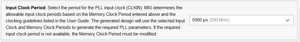
在DDR IP顶层中会有一个sys_clk_i的信号,此信号就代表的是Input Clock Period 。设置的是200MHz,那么需要外部信号提供一个200MHz的时钟。也可以外部提供一个50MHz的时钟,然后通过PLL分频得到一个200MHz的时钟提供给sys_clk_i。
本篇文章仅作为个人学习记录,如有误请大佬指出,谢谢。

